What’s A Switching Transistor?
A Switching Transistor is a transistor which is used as a switch. A transistor is a 3-terminal semiconductor device that can be used for switching applications, amplification of weak signals, and in quantities of thousands and millions of transistors are interconnected and embedded into a tiny integrated circuit (IC), which makes computer memories, like ROM.
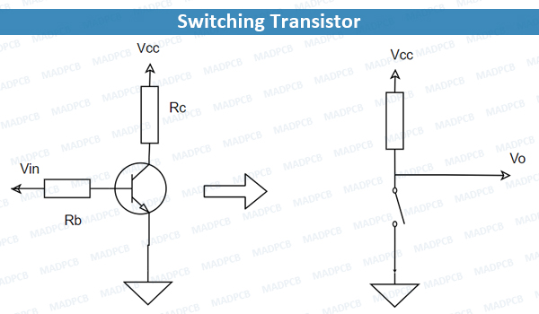
Switching Transistor
A transistor switch, which is used for opening or closing of a circuit, that means the transistor is commonly used as a switch in the electronic devices only for the low voltage applications because of its low power consumption. Transistor work as a switch when it is in cutoff and saturation regions.
Transistor as a Switch
If the circuit uses the BJT transistors as a switch, the biasing of the transistor, either NPN or PNP is arranged to operate the transistor at both sides of the I-V characteristics curves shown below. A transistor can be operated in three modes, active region, saturation region, and cut-off region. In the active region, the transistor works as an amplifier. As a transistor switch, it operates in two regions and those are Saturation Region (fully-ON) and the Cut-off Region (fully-OFF). The transistor as a switch circuit diagram.
Both the types NPN and PNP transistors can be operated as switches, we call them as switching transistors. Few of the applications utilize a power transistor as a switching tool. During this condition, there might be no requirement of using another signal transistor to drive this transistor.
Cut-off Region
The operating conditions of the transistor are zero input base current (IB=0), zero output collector current(Ic=0), and maximum collector voltage (VCE) which results in a large depletion layer and no current flowing through the device.
Therefore, the transistor is switched to “Fully-OFF”. So we can define the cut-off region when using a bipolar transistor as a switch as being, bother the junctions of NPN transistors are reverse biased, VB< 0.7v and Ic=0. Similarly, for PNP transistors, the emitter potential must be –ve with respect to the base of the transistor.
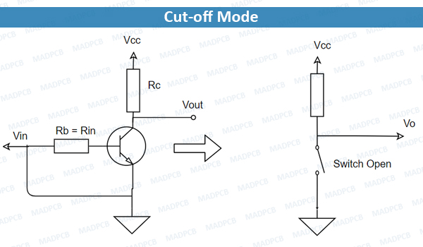
Cut-off Mode
Then we can define the “cut-off region” or “OFF mode” when using a bipolar transistor as a switch as being, both junctions reverse biased, IC = 0, and VB < 0.7v. For a PNP transistor, the Emitter potential must be -ve with respect to the base terminal.
Cut-off Region Characteristics
The characteristics in cut–off region are:
- Both the base and input terminals are grounded which means to ‘0’v
- The voltage level at the base-emitter junction is less than 0.7v
- The base-emitter junction is in reverse biased condition
- Here, the transistor functions as an OPEN switch
- When the transistor is completely OFF, it moves into the cut-off region
- The base-collector junction is in reverse biased condition
- There will be no flow of current in the collector terminal which means Ic = 0
- The voltage value at the emitter-collector junction, and at output terminals is ‘1’
Saturation Region
In this region, the transistor will be biased so that the maximum amount of base current(IB) is applied, resulting in maximum collector current(IC=VCC/RL) and then resulting in the minimum collector-emitter voltage(VCE ~ 0) drop. At this condition, the depletion layer becomes as small as the possible and maximum current flowing through the transistor. Therefore the transistor is switched “Fully-ON”.
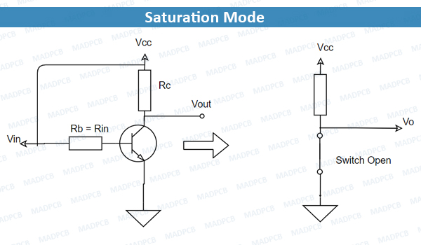
Saturation Mode
The definition of “saturation region” or “ON mode” when using a bipolar NPN transistor as a switch as being, both the junctions are forward biased, IC = Maximum, and VB > 0.7v. For a PNP transistor, the Emitter potential must be +ve with respect to the Base. This is the working of the transistor as a switch.
Saturation Region Characteristics
The saturation characteristics are:
- Both the base and input terminals are connected to Vcc = 5v
- The voltage level at the base-emitter junction is more than 0.7v
- The base-emitter junction is in forward biased condition
- Here, the transistor functions as a CLOSED switch
- When the transistor is completely OFF, it moves into the saturation region
- The base-collector junction is in forward biased condition
- The current flow in the collector terminal is Ic = (Vcc/RL)
- The voltage value at the emitter-collector junction, and at output terminals is ‘0’
- When the voltage at the collector-emitter junction is ‘0’, this means ideal saturation condition
In addition, the working of transistor as a switch can be explained in detail as below:
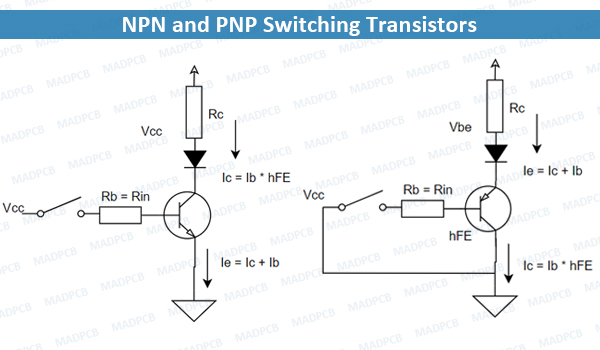
Transistor as a Switch – NPN
Depending on the applied voltage value at the base edge of the transistor, switching functionality takes place. When there is a good amount of voltage which is ~0.7V in between the emitter and the base edges, then the flow of voltage at the collector to emitter edge is zero. So, the transistor in this condition performs as a switch and the current that flows through the collector is considered as the transistor current.
In the same way, when there is no voltage applied at the input terminal, then the transistor functions in the cut-off region and functions as an open circuit. In this switching method, the connected load in contact with the switching point where this acts as a reference point. So, when the transistor moves into the ‘ON’ condition, there will be a flow of current from the source terminal to the ground via load.
To be clear of this switching method, let us consider an example.
Assume that a transistor has a base resistance value of 50kOhm, the resistance at the collector edge is 0.7kOhm and the applied voltage is of 5V and considers beta value as 150. At the base edge, a signal that varies between 0 and 5V is applied. This corresponds that the collector output is observed by modifying the input voltage values which are 0 and 5V. Consider the following diagram.
When VCE = 0, then IC= VCC/RC
IC = 5/0.7
So, current at collector terminal is 7.1mA
As beta value is 150, then Ib = Ic/β
Ib = 7.1/150 = 47.3 µA
So, base current is 47.3 µA
With the above values, the highest value of current at the collector terminal is of 7.1 mA in the condition collector to emitter voltage is zero and the base current value is 47.3 µA. Thus, it got proved that when the value of current at the base edge is enhanced above 47.3 µA, then the NPN transistor moves into the saturation region.
Assume that a transistor has an input voltage of 0V. This means that the base current is ‘0’ and when the emitter junction is grounded, then the emitter and base junction will not be in forwarding bias condition. So, the transistor is in OFF mode and the voltage value at the collector edge is 5V.
Vc= Vcc – (IcRc)
= 5-0
Vc = 5V
Assume that a transistor has an input voltage of 5V. Here, the current value at the base edge can be known by using Kirchhoff’s voltage principle.
Ib = (Vi – Vbe)/Rb
When a silicon transistor is considered, it has Vbe = 0.7V
So, Ib = (5-0.7)/50
Ib = 56.8µA
Thus, it got proved that when the value of current at the base edge is enhanced above 56.8 µA, then the NPN transistor moves into a saturation region at 5V input condition.
NPN and PNP Switching Transistors
Transistor as a Switch – PNP
The switching functionality for both the PNP and NPN transistors are similar but the variation is that in PNP transistor, the flow of current is from the base terminal. This switching configuration is employed for the negative ground connections. Here, the base edge has a negative bias connection in correspondence to the emitter edge. When the voltage at the base terminal is more -ve, then there will be a flow of base current. To be clear, that when a very minimal or -ve voltage valves exist, then this makes the transistor as short-circuited if not open-circuited or else high impedance.
In this type of connection, the load is in connection with the switching output along with a reference point. When the PNP transistor is in ON condition, there will be current flow from source to load and then to ground via a transistor.
As same to NPN transistor switching operation, PNP transistor input is also at the base edge, whereas the emitter terminal is in connection with a fixed voltage and the collector terminal is connected to the ground via a load. The below picture explains the circuit.
Here base terminal is always in a negative bias condition in correspondence to the emitter edge and the base it connected at the negative side and the emitter at the positive side of the input voltage. This means that the voltage at the base to emitter is negative and the voltage at emitter to collector is positive. So, there will be transistor conductivity when the emitter voltage has a more positive level than that of base and collector terminals. Thus, the voltage at the base should be more negative than that of other terminals.
To know the value of collector and base currents, we need the below expressions.
Ic = Ie – Ib
Ic = β. Ib
Where Ub = Ic/β
To be clear of this switching method, let us consider an example.
Assume that the load circuit needs 120 mA and the beta value of the transistor is 120. Then the current value that is needed for the transistor to be in saturation mode is
Ib = Ic/β
= 120 mAmps/100
Ib = 1 mAmp
So, when there is a base current of 1 mAmp, then the transistor is completely in ON condition. Whereas in practical scenarios, approximately 30-40 percent of more current is necessary for proper transistor saturation. This means the base current which is necessary for the device is 1.3 mAmps.
Switching Operation of Darlington Transistor
In a few cases, the current gain of direct current in the BJT device is very minimal for direct switching of the load voltage or current. Because of this, switching transistors are utilized. In this condition, a small transistor device is included for ON and OFF of a switch and an increased value of current for regulating the output transistor.
In order to enhance the signal gain, two transistors are connected in the way of “complementary gain compounding configuration”. In this configuration, the amplification factor is the result of the product of two transistors.
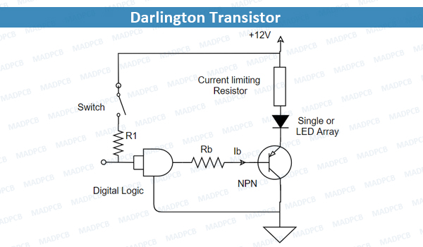
Darlington Transistor
Darlington transistors are usually included with two bipolar PNP and NPN types of transistors where these are connected in the way that the gain value of the initial transistor is multiplied with the gain value of the second transistor device.
This produces the result where the device functions as a single transistor having maximum current gain even for a minimal base current value. The whole current gain of the Darlington switch device is the product of current gain values of both PNP and NPN transistors and this represented as:
β = β1 × β2
With the above points, Darlington transistors having maximum β and collector current values are potentially related to the switching of a single transistor.
For instance, when the input transistor has a current gain value of 100 and the second has a gain value of 50, then the total current gain is
β = 100 × 50 = 5000
So, when the load current is 200 mA, then the current value in the Darlington transistor at the base terminal is 200 mA/5000 = 40 µAmps which a great decrement when compared with the past 1 mAmp for a single device.
Darlington Configurations
There are mainly two configuration types in the Darlington transistor and those are
The switch configuration of the Darlington transistor demonstrates that the collector terminals of the two devices are connected with the emitter terminal of the initial transistor which has a connection with the base edge of the second transistor device. So, the current value at the emitter terminal of the first transistor will form as the input current of the second transistor thus makes it in On condition.
The input transistor which is the first one gets its input signal at the base terminal. The input transistor gets amplified in a general way and this is used to drive the next output transistors. The second device enhances the signal and this results in a maximum value of current gain. One of the crucial features of the Darlington transistor is its maximum current gain when related to the single BJT device.
In addition to the ability of maximum voltage and current switching characteristics, the other added benefit is its maximum switching speeds. This switching operation allows the device to be specifically used for inverter circuits, DC motor, lighting circuits, and stepper motor regulation purposes.
The variation to take into account while utilizing Darlington transistors than that of conventional single BJT types when implementing the transistor as a switch is that the input voltage at the base and emitter junction requires to be more which is nearly 1.4v for silicon type of device, as because of a series connection of the two PN junctions.
Some of the Common Practical Applications of Transistor as a Switch
In a transistor, unless a current flow in the base circuit, there is no current can flow in the collector circuit. This property will allow a transistor to be used as a switch. The transistor can be switched ON or OFF by changing the base. There are a few applications of switching circuits operated by transistors. Here, I considered NPN transistor to explain a few applications which are using transistor switch.
Light-Operated Switch
The circuit is designed by using a transistor as a switch, to light the bulb in a bright environment and to turn it off in the dark and a Light-Dependent Resistor (LDR) in the potential divider. When the environment dark LDR’s resistance becomes high. Then the transistor is switched OFF. When the LDR is exposed to the bright light, its resistance falls to less value resulting in more supply voltage and raising the base current of the transistor. Now the transistor is switched ON, the collector current flows and the bulb lights up.
Heat-Operated Switch
One important component in the circuit of a heat-operated switch is the thermistor. The thermistor is a type of resistor that responds depending upon the surrounding temperature. Its resistance increases when the temperature is low and vice versa. When heat is applied to the thermistor, its resistance drops and the base current increases followed by a greater increase in the collector current and the siren will blow. This particular circuit is suitable as a fire alarm system.
DC Motor Control (driver) in the Case of High Voltages
Consider no voltage is applied to the transistor, then the transistor becomes OFF and no current will flow through it. Hence the relay remains in OFF state. Power to the DC motor is fed from the Normally Closed (NC) terminal of the relay, so the motor will rotate when the relay is in OFF state. The apply to high voltage at the base of transistor BC548 causes turning ON of the transistor and the relay coil to energize.
Practical Example
Here, we are going to know the value of the base current that is required to make a transistor completely into ON condition where the load needs a current of 200mA when the input value is enhanced to 5v. Also, know the value of Rb.
The base current value of transistor is
Ib = Ic/β consider β = 200
Ib = 200mA/200 = 1mA
The base resistance value of the transistor is Rb = (Vin – Vbe)/Ib
Rb = (5 – 0.7)/1 × 10-3
Rb = 4.3kΩ
Transistor switches are widely employed in multiple applications like interfacing huge current or high value of voltage equipment such as motors, relays, or lights to the minimal value of voltage, digital IC’s or used in logical gates such as AND gates or OR. Also, when the output delivered from the logic gate is +5v whereas the device that has to be regulated might need wither 12v or even 24v of the supply voltage.
Or the load like DC Motor might require to have its speed monitored through some continuous pulses. Transistor switches permit this operation to be quicker and more simply than compared with that of traditional mechanical switches.
Why Use Transistor Instead of Switch?
While implementing a transistor in the place of a switch, even a minimal amount of base current regulates a higher load current in the collector terminal. Using transistors in the place of switch, these devices are supported with relays and solenoids. Whereas in the case when higher levels of currents or voltages are to be regulated, then Darlington transistors are utilized.
On the whole, as a summary, few of the conditions that are applied while operating transistor as a switch are
- While making use of BJT as a switch, then has to be operated either incomplete ON or complete ON conditions.
- While using a transistor as a switch, a minimal value of base current regulates increased collector load current.
- While implementing transistors to switch as relays and solenoids, then it is better to use flywheel diodes.
- To regulate larger values of either voltage or currents, the Darlington transistors work at best.