Understanding the Significance and Pros and Cons of PCB Copper Pour
Charles Liu
Electronics engineer | PCB&PCBA one-stop solution | Components sourcing | Hardware
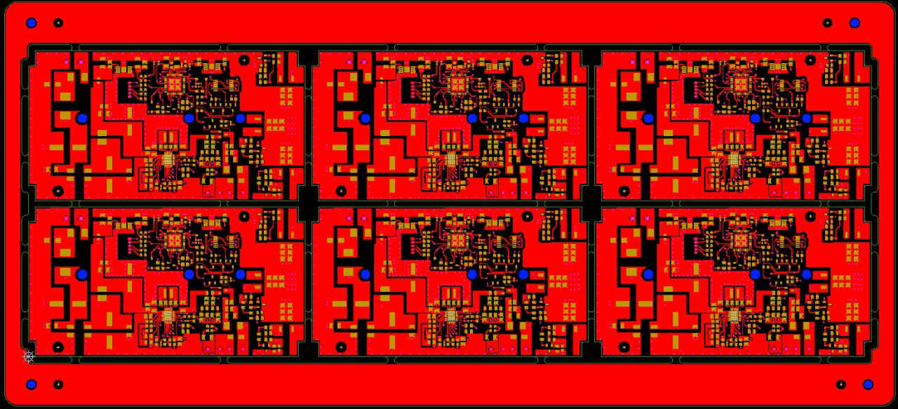
PCB copper pour is a critical aspect of circuit board design. It involves filling the unused space in non-routed areas of the PCB with solid copper. The significance of copper pour lies in reducing ground impedance, enhancing immunity to interference, lowering voltage drops to boost power efficiency, and connecting to ground to minimize loop areas.
Significance of PCB Copper Pour
The primary benefit of copper pour is the reduction of ground impedance, which is crucial for digital circuits that often encounter high-frequency pulse currents. Thus, reducing ground impedance is deemed necessary.
It is generally believed that circuits composed entirely of digital devices should have large ground planes. However, for analog circuits, the ground loop formed by copper pouring may cause electromagnetic coupling interference, which outweighs the benefits (except for high-frequency PCB circuits). Therefore, not all circuits require copper pouring.
Pros and Cons of PCB Copper Pour
Pros
For EMC (Electromagnetic Compatibility) requirements, large ground or power planes shielded by copper pouring offer protection. Some special grounds, such as PGND (Protective Ground), serve a protective role.
For PCB manufacturing process requirements, to ensure uniform copper plating or to prevent lamination deformation, copper pouring is applied to PCBs with fewer traces.
For signal integrity requirements, copper pouring provides a complete return path for high-frequency digital signals and reduces the need for DC network wiring. Additionally, it aids in heat dissipation and meets special device installation requirements.
Cons
Fully covering component pins with copper may lead to excessive heat dissipation, making desoldering and rework difficult. To avoid this, components are sometimes connected in a cross shape (pins and pads form a "cross").
Copper pouring around antenna parts may weaken signals, leading to signal interference and affecting the performance of amplification circuits. Therefore, the area around antenna parts is generally not copper-poured.
Shapes of PCB Copper Pour
Solid Shape Copper Pour
Solid copper pouring serves both as a current amplifier and a shield. However, during wave soldering, solid copper plating may cause the board to warp or even bubble due to thermal expansion and contraction forces. Therefore, solid copper pouring typically includes several slots to relieve stress and prevent copper foil bubbling.
Grid Shape Copper Pour
Grid copper pouring primarily acts as a shield, with its current amplification effect reduced. From a heat dissipation perspective, grid copper pouring reduces the heated area of the copper while providing a certain degree of electromagnetic shielding. However, the production process imposes certain requirements on the grid-shaped copper pour, as overly small grids can impact quality and yield.
PCB Copper Pour Design
In PCB design, each side of the PCB is generally covered with copper to ground. This is mainly to prevent PCB bending and various signal interference and crosstalk.
Therefore, during routing, copper should be poured to ground. However, due to the large number of components and traces on the outer layer, the copper foil is divided into many small isolated copper islands and thin copper foil.
Handling Broken Copper
Long, isolated, and poorly grounded copper areas can act as antennas, causing EMC issues. Therefore, it is advisable to avoid generating broken copper during copper pouring. If broken copper occurs, it should be removed.
Handling Isolated Copper
Isolated (dead) copper islands, if small, are equivalent to broken copper and can be removed. If they are large, they can be defined as a certain ground and treated with added vias, eliminating the isolated copper.
PADS Copper Pouring in Gerber Files
For PADS-designed files, copper pouring needs to be reapplied every time the file is reopened, as PADS software uses linear copper foil, which is a characteristic of PADS software. Linear copper foil data is large, so reopening a saved copper pour after closing the software will be slow and laggy. Therefore, after closing the PADS software, only the copper foil outline of the design file is retained.
DFM Inspection of Copper Pour Design
Regarding the manufacturability issues of broken copper and isolated copper, during the production process, broken copper is etched away due to its elongated characteristics, causing the copper to separate and fall off in other locations, resulting in different network short circuits.
When CAM engineers at the board manufacturer handle production files, they will ask for clarification from the design engineer regarding isolated copper, as isolated copper without network links is an abnormal design. Therefore, the presence of isolated copper in the design will waste communication costs and delay the production cycle.