


Kicad Tutorial: Copper pours / fills
This is part of a series of short tutorials on advanced topics of using Kicad, the favorite schematic/PCB design software here at Wayne and Layne.
A copper pour or fill refers to an area on a printed circuit board where the original copper is not etched away, and remains in place, usually electrically connected to the Ground signal, producing a “Ground Plane”. This has a number of advantages, including decreasing the amount of etching fluid required during manufacturing, as well as reducing the amount of electrical noise and signal crosstalk experienced by the circuit elements.
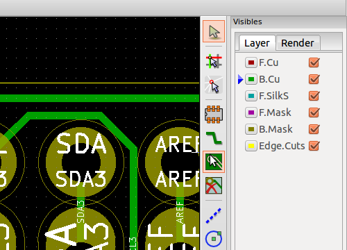
It is relatively easy to create a copper fill in Kicad. We usually add fills after having already drawn in the PCB outline in the Edges layer. First, ensure that you have selected one of the copper layers (such as “Front†or “F.Cuâ€). Then, select the “Add Filled Zones†from the toolbar on the right side of the screen.
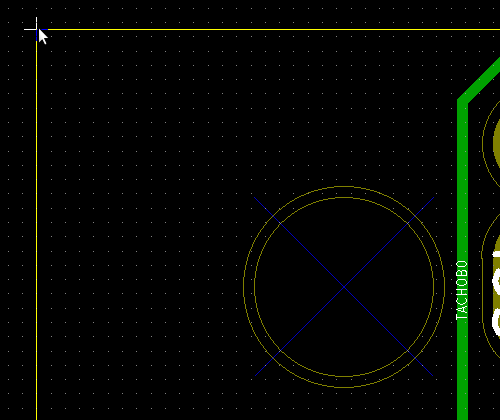
Next, click in one corner of the PCB outline to start drawing the copper fill.
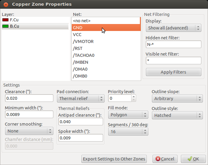
Once you click in the first corner, the following properties box will appear. Select the relevant copper layer (here, either “F.Cu” or “B.Cu”) and the desired net for the fill (usually you want “GND”, but sometimes you might want some other net, or “<no net>” which will make an isolated copper fill). The settings in the bottom half are important for controlling the drawing of the filled area as well as the “thermals”. One potential problem with adding ground fill is that the ground pads will become very difficult to solder, as the ground plane will suck away all the heat from your soldering iron, and the pad won’t ever heat up hot enough for the solder to flow. To avoid this problem, you almost always want to add “thermal relief” to your ground pads, which means there is a keep-out area adjacent to each ground pad where there is no fill, and instead each ground pad is connected by a number of thinner traces. This still provides a very good electrical connection for the ground pad, but makes it much easier to solder. The “Clearance” setting controls the general clearance between the filled area and pads/traces of other nets. The “Minimum width” setting controls the thinnest that the fill can be when flowing around other pads/traces. The “Thermal Reliefs” settings control the clearance around the ground pads (0.040″ here) and the width of the traces connecting from the fill to the ground pads (0.009″ here). We’ve found these settings to work pretty well for most of our projects. You also want to select “Arbitrary” for the “Outline Slope” setting to make it easier to draw the zone outline. Click “OK” to close this window and continue drawing the fill outline. (Click the image to enlarge)
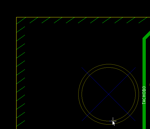
Once you have closed the zone properties window, click once in each of the other three corners (in order) on the board outline. Then, to complete the final segment, double-click on the original corner to end the zone. You should see red or green hatching (depending on which copper layer you used) on the edges of your PCB indicating the filled region, as shown in the image below.
Generally you want to have a copper fill on both the top and bottom of the PCB. To add the fill on the other side, the easiest way is to right-click on the existing board edge, select “Zone outline”, then go to “Zones”->”Duplicate Zone”. This brings up the zone properties box for the new zone, so select the other copper layer and press “OK”.
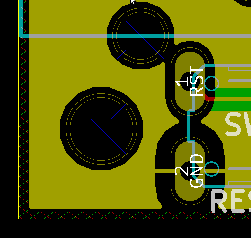
To see the copper fills in your design, click on the “Show filled areas in zones” button, the 10th button in the left-size toolbar. The button below that will hide the fills. Then, you can run the DRC tool (Ladybug Checkmark in the top toolbar) which will fill all your zones. You should see something like the image below. The brown-yellow color is the combination of red (top side) and green (bottom side) copper fills. We can see the 20 mil clearance between the fill and non-ground copper, and the larger 40 mil clearance between the fill and GND pads.
Other tutorials in this series:
Slight correction:
“The settings in the bottom half are *import* for …”
I guess you meant “important”.
Thanks for the excellent tutorial!
If you want to connect filled zones on both sides of a 2 layer board together, take a look at https://bugs.launchpad.net/kicad/+bug/999057/comments/4
It’s a hack but it’s the cleanest way of doing this as of now.
László, thank you very much for the comment and the compliments, I have updated fixed the “import” into “important”. Glad you liked the tutorial!
Mansour, that is a very useful link, thanks for sharing!
Text “First, select the proper tool from the toolbar on the right side of the screen. Also, ensure that you have selected one of the copper layers (such as “Front†or “F.Cuâ€).”, would be more helpful if it were written as sequential operations (in this case, “First” is not first); and specify the tool since it can be known in advance:
“First, ensure that you have selected one of the copper layers (such as “Front†or “F.Cuâ€). Then, select the “Add Filled Zones” from the toolbar on the right side of the screen.”, etc.
Also, Text “To add the fill on the other side, the easiest way is to right-click on the board edge,” should read “To add the fill on the other side, the easiest way is to right-click on the EXISTING ZONE edge,”, etc.
Thanks for this helpful tutorial.
Hi Dan, thanks for the suggested tweaks to the wording to reduce confusion. I have updated the text of this post to improve understanding as you suggested. Thanks again! -Layne
Delete a filled zone with mouse over one of the edge segments and hit Del.
Hi Layne,
Any way to add restrict zones (like in Eagle) to stop kicad from filling certain areas with copper without having a component there?
Good tutorial!
Hi Giovanni, good question. There is a way to do this. Right-click on the zone outline, then select “Zones” -> “Add Cutout Area”. Now you can use the cursor to define a closed region that will be subtracted from the current zone. You can use this multiple times to create multiple keep-out areas in your fill. Hope that helps!
Thank you very much for this! 🙂
there is something seriously overlooked here.
I have multiple nets as a polygon, then when I make a copper pour, it will run straight into another polygon net.
this is terrible. can someone explain how this is even possible?
hey is this like a test pad in the terms of it being exsposed.
Hi Liam, making a copper fill region will not affect the soldermask that is typically overlaid on top of the copper, so it will not make a test pad. You should probably add a test pad component to your schematic and map it to a simple circle pad footprint, if that’s what you’re trying to do. Good luck!