TDA7560 - Datasheet Catalog
TDA7560 - Datasheet Catalog
TDA7560 - Datasheet Catalog

Create successful ePaper yourself
Turn your PDF publications into a flip-book with our unique Google optimized e-Paper software.
®<br />
<strong>TDA7560</strong><br />
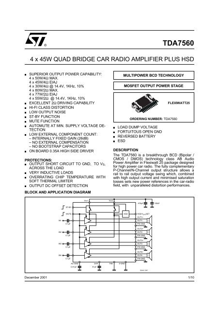
4 x 45W QUAD BRIDGE CAR RADIO AMPLIFIER PLUS HSD<br />
SUPERIOR OUTPUT POWER CAPABILITY:<br />
4 x 50W/4Ω MAX.<br />
4 x 45W/4Ω EIAJ<br />
4 x 30W/4Ω @ 14.4V, 1KHz, 10%<br />
4 x 80W/2Ω MAX.<br />
4 x 77W/2Ω EIAJ<br />
4 x 55W/2Ω @ 14.4V, 1KHz, 10%<br />
EXCELLENT 2Ω DRIVING CAPABILITY<br />
HI-FI CLASS DISTORTION<br />
LOW OUTPUT NOISE<br />
ST-BY FUNCTION<br />
MUTE FUNCTION<br />
AUTOMUTE AT MIN. SUPPLY VOLTAGE DE-<br />
TECTION<br />
LOW EXTERNAL COMPONENT COUNT:<br />
– INTERNALLY FIXED GAIN (26dB)<br />
– NO EXTERNAL COMPENSATION<br />
– NO BOOTSTRAP CAPACITORS<br />
ON BOARD 0.35A HIGH SIDE DRIVER<br />
PROTECTIONS:<br />
OUTPUT SHORT CIRCUIT TO GND, TO VS,<br />
ACROSS THE LOAD<br />
VERY INDUCTIVE LOADS<br />
OVERRATING CHIP TEMPERATURE WITH<br />
SOFT THERMAL LIMITER<br />
OUTPUT DC OFFSET DETECTION<br />
BLOCK AND APPLICATION DIAGRAM<br />
MULTIPOWER BCD TECHNOLOGY<br />
MOSFET OUTPUT POWER STAGE<br />
ORDERING NUMBER: <strong>TDA7560</strong><br />
LOAD DUMP VOLTAGE<br />
FORTUITOUS OPEN GND<br />
REVERSED BATTERY<br />
ESD<br />
FLEXIWATT25<br />
DESCRIPTION<br />
The <strong>TDA7560</strong> is a breakthrough BCD (Bipolar /<br />
CMOS / DMOS) technology class AB Audio<br />
Power Amplifier in Flexiwatt 25 package designed<br />
for high power car radio. The fully complementary<br />
P-Channel/N-Channel output structure allows a<br />
rail to rail output voltage swing which, combined<br />
with high output current and minimised saturation<br />
losses sets new power references in the car-radio<br />
field, with unparalleled distortion performances.<br />
Vcc1<br />
Vcc2<br />
470µF<br />
100nF<br />
ST-BY<br />
MUTE<br />
HSD<br />
HSD/V OFF DET<br />
OUT1+<br />
IN1<br />
OUT1-<br />
0.1µF<br />
PW-GND<br />
OUT2+<br />
IN2<br />
OUT2-<br />
0.1µF<br />
PW-GND<br />
OUT3+<br />
IN3<br />
OUT3-<br />
0.1µF<br />
PW-GND<br />
OUT4+<br />
IN4<br />
OUT4-<br />
0.1µF<br />
PW-GND<br />
AC-GND<br />
SVR TAB S-GND<br />
0.47µF 47µF<br />
D94AU158C<br />
December 2001<br />
1/10
<strong>TDA7560</strong><br />
ABSOLUTE MAXIMUM RATINGS<br />
Symbol Parameter Value Unit<br />
V CC Operating Supply Voltage 18 V<br />
V CC (DC) DC Supply Voltage 28 V<br />
V CC (pk) Peak Supply Voltage (t = 50ms) 50 V<br />
I O<br />
Output Peak Current:<br />
Repetitive (Duty Cycle 10% at f = 10Hz)<br />
Non Repetitive (t = 100µs)<br />
P tot Power dissipation, (T case = 70°C) 80 W<br />
T j Junction Temperature 150 °C<br />
T stg Storage Temperature – 55 to 150 °C<br />
9<br />
10<br />
A<br />
A<br />
PIN CONNECTION (Top view)<br />
1 25<br />
TAB<br />
P-GND2<br />
ST-BY<br />
OUT2+<br />
P-GND1<br />
OUT1+<br />
SVR<br />
IN1<br />
IN2<br />
S-GND<br />
IN4<br />
IN3<br />
AC-GND<br />
OUT3+<br />
P-GND3<br />
VCC<br />
OUT4+<br />
MUTE<br />
OUT2-<br />
VCC<br />
OUT1-<br />
OUT3-<br />
OUT4-<br />
P-GND4<br />
HSD<br />
D94AU159A<br />
THERMAL DATA<br />
Symbol Parameter Value Unit<br />
R th j-case Thermal Resistance Junction to Case Max. 1 °C/W<br />
2/10
ELECTRICAL CHARACTERISTICS (VS = 13.2V; f = 1KHz; Rg = 600Ω; RL = 4Ω; Tamb = 25°C;<br />
Refer to the test and application diagram, unless otherwise specified.)<br />
Symbol Parameter Test Condition Min. Typ. Max. Unit<br />
I q1 Quiescent Current R L = ∞ 120 200 320 mA<br />
V OS Output Offset Voltage Play Mode ±60 mV<br />
dV OS During mute ON/OFF output<br />
±60 mV<br />
offset voltage<br />
G v Voltage Gain 25 26 27 dB<br />
dG v Channel Gain Unbalance ±1 dB<br />
P o Output Power V S = 13.2V; THD = 10%<br />
V S = 13.2V; THD = 1%<br />
V S = 14.4V; THD = 10%<br />
V S = 14.4V; THD = 1%<br />
V S = 13.2V; THD = 10%, 2Ω<br />
V S = 13.2V; THD = 1%, 2Ω<br />
V S = 14.4V; THD = 10%, 2Ω<br />
V S = 14.4V; THD = 1%, 2Ω<br />
P o EIAJ EIAJ Output Power (*) V S = 13.7V; R L = 4Ω<br />
V S = 13.7V; R L = 2Ω<br />
P o max. Max. Output Power (*) V S = 14.4V; R L = 4Ω<br />
V S = 14.4V; R L = 2Ω<br />
THD Distortion P o = 4W<br />
P o = 15W; R L = 2Ω<br />
e No Output Noise "A" Weighted<br />
Bw = 20Hz to 20KHz<br />
23<br />
16<br />
28<br />
20<br />
42<br />
32<br />
50<br />
40<br />
25<br />
19<br />
30<br />
23<br />
45<br />
34<br />
55<br />
43<br />
41 45<br />
77<br />
50<br />
80<br />
0.006<br />
0.015<br />
35<br />
50<br />
0.05<br />
0.07<br />
50<br />
70<br />
SVR Supply Voltage Rejection f = 100Hz; V r = 1Vrms 50 70 dB<br />
f ch High Cut-Off Frequency P O = 0.5W 100 300 KHz<br />
R i Input Impedance 80 100 120 KΩ<br />
C T Cross Talk f = 1KHz P O = 4W<br />
60 70 – dB<br />
f = 10KHz P O = 4W<br />
60 – dB<br />
I SB St-By Current Consumption V St-By = 1.5V 75 µA<br />
I pin4 St-by pin Current VSt-By = 1.5V to 3.5V ±10 µA<br />
V SB out St-By Out Threshold Voltage (Amp: ON) 3.5 V<br />
V SB in St-By in Threshold Voltage (Amp: OFF) 1.5 V<br />
A M Mute Attenuation P Oref = 4W 80 90 dB<br />
V M out Mute Out Threshold Voltage (Amp: Play) 3.5 V<br />
V M in Mute In Threshold Voltage (Amp: Mute) 1.5 V<br />
V AM in V S Automute Threshold (Amp: Mute)<br />
Att ≥ 80dB; P Oref = 4W<br />
(Amp: Play)<br />
6.5 7<br />
V<br />
Att < 0.1dB; P O = 0.5W<br />
7.5 8 V<br />
I pin22 Muting Pin Current V MUTE = 1.5V<br />
7 12 18 µA<br />
(Sourced Current)<br />
V MUTE = 3.5V -5 18 µA<br />
HSD SECTION<br />
V dropout Dropout Voltage IO = 0.35A; VS = 9 to 16V 0.25 0.6 V<br />
I prot Current Limits 400 800 mA<br />
OFFSET DETECTOR SECTION<br />
V M_ON Mute Voltage for DC offset V stby = 5V 8 V<br />
V M_OFF<br />
detection enabled<br />
6 V<br />
V OFF Detected Differential Output Offset V stby = 5V; V mute = 8V ±2 ±3 ±4 V<br />
V 25_T Pin 25 Voltage for Detection =<br />
TRUE<br />
V stby = 5V; V mute = 8V<br />
V OFF > ±4V<br />
0 1.5 V<br />
V 25_F Pin 25 Voltage for Detection =<br />
FALSE<br />
(*) Saturated square wave output.<br />
V stby = 5V; V mute = 8V<br />
V OFF > ±2V<br />
<strong>TDA7560</strong><br />
W<br />
W<br />
W<br />
W<br />
W<br />
W<br />
W<br />
W<br />
W<br />
W<br />
W<br />
W<br />
%<br />
%<br />
µV<br />
µV<br />
12 V<br />
3/10
<strong>TDA7560</strong><br />
Figure 1: Standard Test and Application Circuit<br />
C8<br />
0.1µF<br />
C7<br />
2200µF<br />
Vcc1-2<br />
Vcc3-4<br />
ST-BY<br />
MUTE<br />
IN1<br />
R1<br />
10K<br />
R2<br />
47K<br />
C1<br />
0.1µF<br />
C9<br />
1µF<br />
C10<br />
1µF<br />
4<br />
22<br />
11<br />
6 20<br />
9<br />
8<br />
7<br />
5<br />
2<br />
3<br />
OUT1<br />
OUT2<br />
IN2<br />
12<br />
17<br />
C2 0.1µF<br />
18<br />
OUT3<br />
IN3<br />
15<br />
19<br />
C3 0.1µF<br />
21<br />
IN4<br />
14<br />
24<br />
OUT4<br />
C4 0.1µF<br />
S-GND<br />
13<br />
16 10 25 1<br />
23<br />
C5<br />
0.47µF<br />
SVR<br />
C6<br />
47µF<br />
HSD<br />
TAB<br />
D95AU335B<br />
4/10
<strong>TDA7560</strong><br />
Figure 2: P.C.B. and component layout of the figure 1 (1:1 scale)<br />
COMPONENTS &<br />
TOP COPPER LAYER<br />
BOTTOM COPPER LAYER<br />
5/10
<strong>TDA7560</strong><br />
Figure 3. Quiescent current vs. supply<br />
voltage.<br />
240 Id (mA) Vi = 0<br />
220<br />
200<br />
180<br />
160<br />
RL = 4 Ohm<br />
140<br />
8 10 12 14 16 18<br />
Vs (V)<br />
Figure 4. Output power vs. supply voltage.<br />
Po (W)<br />
80<br />
75<br />
Po-max<br />
70<br />
65<br />
60 RL= 4 Ohm<br />
55 f= 1 KHz<br />
50<br />
THD= 10 %<br />
45<br />
40<br />
35<br />
30<br />
25<br />
20<br />
THD= 1 %<br />
15<br />
10<br />
5<br />
8 9 10 11 12 13 14 15 16 17 18<br />
Vs (V)<br />
Figure 5. Output power vs. supply voltage.<br />
Po (W)<br />
130<br />
120<br />
Po-max<br />
110<br />
100<br />
90<br />
RL= 2 Ohm<br />
f= 1 KHz THD= 10 %<br />
80<br />
70<br />
60<br />
50<br />
40<br />
THD= 1 %<br />
30<br />
20<br />
10<br />
8 9 10 11 12 13 14 15 16 17 18<br />
Vs (V)<br />
Figure 7. Distortion vs. output power<br />
Figure 6. Distortion vs. output Power<br />
10 THD (%) Vs= 14.4 V<br />
1<br />
RL = 4 Ohm<br />
f = 10 KHz<br />
0.1<br />
0.01<br />
f = 1 KHz<br />
0.001<br />
0.1 1 10<br />
Po (W)<br />
Figure 8. Distortion vs. frequency.<br />
10<br />
THD (%)<br />
1<br />
10 THD (%) f = 10 KHz<br />
Vs= 14.4 V<br />
RL = 2 Ohm<br />
1<br />
Vs = 14.4 V<br />
RL = 4 Ohm<br />
Po = 4 W<br />
0.1<br />
0.1<br />
0.01<br />
f = 1 KHz<br />
0.01<br />
0.001<br />
0.1 1 10<br />
Po (W)<br />
6/10<br />
0.001<br />
10 100 1000 10000<br />
f (Hz)
<strong>TDA7560</strong><br />
Figure 9. Distortion vs. frequency.<br />
THD (%)<br />
10<br />
Figure 10. Crosstalk vs. frequency.<br />
CROSSTALK (dB)<br />
90<br />
1<br />
0.1<br />
0.01<br />
Vs = 14.4 V<br />
RL = 2 Ohm<br />
Po = 8 W<br />
80<br />
70<br />
60<br />
50<br />
40<br />
30<br />
RL = 4 Ohm<br />
Po = 4 W<br />
Rg = 600 Ohm<br />
0.001<br />
10 100 1000 10000<br />
f (Hz)<br />
20<br />
10 100 1000 10000<br />
f (Hz)<br />
Figure 11. Supply voltage rejection vs. frequency.<br />
SVR (dB)<br />
100<br />
90<br />
80<br />
70<br />
60<br />
50<br />
Rg= 600 Ohm<br />
40 Vripple= 1 Vrms<br />
30<br />
20<br />
10 100 1000 10000<br />
f (Hz)<br />
Figure 12. Output attenuation vs. supply<br />
voltage.<br />
0<br />
-20<br />
-40<br />
-60<br />
-80<br />
OUT ATTN (dB)<br />
RL = 4 Ohm<br />
Po= 4 W ref.<br />
-100<br />
5 6 7 8 9 10<br />
Vs (V)<br />
Figure 13. Output noise vs. source resistance.<br />
130<br />
120<br />
110<br />
100<br />
En (uV)<br />
Vs= 14.4 V<br />
RL= 4 Ohm<br />
90<br />
80<br />
70<br />
60<br />
22-22 KHz lin.<br />
50<br />
40<br />
"A" wgtd<br />
30<br />
20<br />
1 10 100 1000<br />
Rg (Ohm)<br />
10000 100000<br />
Figure 14. Power dissipation & efficiency vs.<br />
output power (sine-wave operation)<br />
90 Ptot (W) n (%)<br />
90<br />
80<br />
n<br />
80<br />
70<br />
60<br />
Vs= 13.2 V<br />
RL= 4 x 4 Ohm<br />
f= 1 KHz SINE<br />
70<br />
60<br />
50<br />
50<br />
40<br />
40<br />
30<br />
Ptot<br />
30<br />
20<br />
20<br />
10<br />
10<br />
0<br />
0 2 4 6<br />
0<br />
8 10 12 14 16 18 20 22 24 26 28 30<br />
Po (W)<br />
7/10
<strong>TDA7560</strong><br />
Figure 15. Power dissipation vs. ouput power<br />
(Music/Speech Simulation)<br />
30<br />
25<br />
20<br />
15<br />
10<br />
5<br />
Ptot (W)<br />
Vs= 13.2 V<br />
RL= 4 x 4 Ohm<br />
GAUSSIAN NOISE<br />
CLIP START<br />
0 1 2 3 4 5 6<br />
Po (W)<br />
DC OFFSET DETECTOR<br />
The <strong>TDA7560</strong> integrates a DC offset detector to<br />
avoid that an anomalous DC offset on the inputs<br />
of the amplifier may be multiplied by the gain and<br />
result in a dangerous large offset on the outputs<br />
which may lead to speakers damage for overheating.<br />
The feature is enabled by the MUTE pin and<br />
works with the amplifier umuted and with no signal<br />
on the inputs. The DC offset detection is signaled<br />
out on the HSD pin.<br />
APPLICATION HINTS (ref. to the circuit of fig. 1)<br />
SVR<br />
Besides its contribution to the ripple rejection, the<br />
SVR capacitor governs the turn ON/OFF time sequence<br />
and, consequently, plays an essential role<br />
in the pop optimization during ON/OFF transients.To<br />
conveniently serve both needs, ITS<br />
MINIMUM RECOMMENDED VALUE IS 10µF.<br />
INPUT STAGE<br />
The <strong>TDA7560</strong>’s inputs are ground-compatible and<br />
can stand very high input signals (± 8Vpk) without<br />
any performances degradation.<br />
If the standard value for the input capacitors<br />
(0.1µF) is adopted, the low frequency cut-off will<br />
amount to 16 Hz.<br />
Figure 16. Power dissipation vs. output power<br />
(Music/Speech Simulation)<br />
60<br />
55<br />
50<br />
45<br />
40<br />
35<br />
30<br />
25<br />
20<br />
Ptot (W)<br />
Vs= 13.2 V<br />
RL= 4 x 2 Ohm<br />
GAUSSIAN NOISE<br />
CLIP START<br />
15<br />
10<br />
5<br />
0 2 4 6 8 10<br />
Po (W)<br />
STAND-BY AND MUTING<br />
STAND-BY and MUTING facilities are both<br />
CMOS-COMPATIBLE. In absence of true CMOS<br />
ports or microprocessors, a direct connection to<br />
Vs of these two pins is admissible but a 470<br />
kOhm equivalent resistance should present<br />
between the power supply and the muting and<br />
stand-by pins.<br />
R-C cells have always to be used in order to<br />
smooth down the transitions for preventing any<br />
audible transient noises.<br />
About the stand-by, the time constant to be assigned<br />
in order to obtain a virtually pop-free transition<br />
has to be slower than 2.5V/ms.<br />
HEATSINK DEFINITION<br />
Under normal usage (4 Ohm speakers) the<br />
heatsink’s thermal requirements have to be deduced<br />
from fig. 15, which reports the simulated<br />
power dissipation when real music/speech programmes<br />
are played out. Noise with gaussiandistributed<br />
amplitude was employed for this simulation.<br />
Based on that, frequent clipping occurence<br />
(worst-case) will cause Pdiss = 26W. Assuming<br />
Tamb = 70°C and TCHIP = 150°C as boundary<br />
conditions, the heatsink’s thermal resistance<br />
should be approximately 2°C/W. This would avoid<br />
any thermal shutdown occurence even after longterm<br />
and full-volume operation.<br />
8/10
<strong>TDA7560</strong><br />
DIM.<br />
mm<br />
inch<br />
MIN. TYP. MAX. MIN. TYP. MAX.<br />
A 4.45 4.50 4.65 0.175 0.177 0.183<br />
B 1.80 1.90 2.00 0.070 0.074 0.079<br />
C 1.40 0.055<br />
D 0.75 0.90 1.05 0.029 0.035 0.041<br />
E 0.37 0.39 0.42 0.014 0.015 0.016<br />
F (1) 0.57 0.022<br />
G 0.80 1.00 1.20 0.031 0.040 0.047<br />
G1 23.75 24.00 24.25 0.935 0.945 0.955<br />
H (2) 28.90 29.23 29.30 1.138 1.150 1.153<br />
H1 17.00 0.669<br />
H2 12.80 0.503<br />
H3 0.80 0.031<br />
L (2) 22.07 22.47 22.87 0.869 0.884 0.904<br />
L1 18.57 18.97 19.37 0.731 0.747 0.762<br />
L2 (2) 15.50 15.70 15.90 0.610 0.618 0.626<br />
L3 7.70 7.85 7.95 0.303 0.309 0.313<br />
L4 5 0.197<br />
L5 3.5 0.138<br />
M 3.70 4.00 4.30 0.145 0.157 0.169<br />
M1 3.60 4.00 4.40 0.142 0.157 0.173<br />
N 2.20 0.086<br />
O 2 0.079<br />
R 1.70 0.067<br />
R1 0.5 0.02<br />
R2 0.3 0.12<br />
R3 1.25 0.049<br />
R4 0.50 0.019<br />
V<br />
5˚ (Typ.)<br />
V1<br />
3˚ (Typ.)<br />
V2<br />
20˚ (Typ.)<br />
V3<br />
45˚ (Typ.)<br />
(1): dam-bar protusion not included<br />
(2): molding protusion included<br />
OUTLINE AND<br />
MECHANICAL DATA<br />
Flexiwatt25<br />
V3<br />
H3<br />
H<br />
H1<br />
H2<br />
A<br />
O<br />
R3<br />
L2<br />
L3 L4<br />
N<br />
R4<br />
V2<br />
R<br />
R2<br />
L<br />
L1<br />
V1<br />
V1<br />
R2<br />
R1<br />
D<br />
L5 R1 R1<br />
V<br />
G<br />
G1<br />
F<br />
M<br />
E<br />
M1<br />
B<br />
C<br />
V<br />
FLEX25ME<br />
9/10
<strong>TDA7560</strong><br />
Information furnished is believed to be accurate and reliable. However, STMicroelectronics assumes no responsibility for the consequences<br />
of use of such information nor for any infringement of patents or other rights of third parties which may result from its use. No license is<br />
granted by implication or otherwise under any patent or patent rights of STMicroelectronics. Specification mentioned in this publication are<br />
subject to change without notice. This publication supersedes and replaces all information previously supplied. STMicroelectronics products<br />
are not authorized for use as critical components in life support devices or systems without express written approval of STMicroelectronics.<br />
The ST logo is a registered trademark of STMicroelectronics<br />
© 2001 STMicroelectronics – Printed in Italy – All Rights Reserved<br />
STMicroelectronics GROUP OF COMPANIES<br />
Australia - Brazil - Canada - China - Finland - France - Germany - Hong Kong - India - Israel - Italy - Japan - Malaysia - Malta - Morocco -<br />
Singapore - Spain - Sweden - Switzerland - United Kingdom - United States.<br />
http://www.st.com<br />
10/10
This datasheet has been download from:<br />
www.datasheetcatalog.com<br />
<strong>Datasheet</strong>s for electronics components.